
Thermal Via Configurations and Design Parameters
When designing LED PCB vias, especially for high-power applications, getting the thermal via setup right is critical to managing heat and ensuring reliability. Let’s break down the key parameters you should focus on:
Optimal Via Geometry
- Hole Diameter: Aim for a diameter between 0.3mm and 0.5mm.
- Smaller holes help prevent solder wicking during reflow.
- Larger holes may reduce plating quality and increase thermal resistance.
- Drill-to-Copper Clearance
- Maintain at least 0.1mm clearance to avoid copper slivers during drilling.
- Ensures effective plating and mechanical strength of the via walls.
| Parameter | Recommended Range |
|---|---|
| Via Hole Diameter | 0.3mm – 0.5mm |
| Drill-to-Copper Clearance | ≥ 0.1mm |
Via Array Patterns
Proper layout of vias influences how heat spreads from the LED junction:
- Hexagonal or Grid Arrays
- Provide uniform heat dissipation across the PCB.
- Choose pattern based on space and thermal needs.
- Thermal Resistance Calculation
- Total thermal resistance decreases as via count increases.
- Use formula:
[
R{th_total} = frac{R{th_single}}{N}
]
where N = number of vias.
- Plan arrays to balance thermal efficiency and board real estate.
Plating Specifications
Copper plating quality directly affects via reliability and current capacity:
- Copper Wall Thickness
- IPC-6012 Class 2: Minimum 10 µm plating thickness.
- IPC-6012 Class 3: Enhanced plating >13 µm for higher reliability in LED PCB vias.
- Impact on Current Capacity
- Thicker plating (e.g., 35µm vs. 25µm) improves current handling and reduces resistance.
- Enhanced plating also strengthens thermal conduction paths.
| Plating Class | Copper Thickness (µm) | Use Case |
|---|---|---|
| IPC-6012 Class 2 | ≥ 10 µm | General LED PCBs |
| IPC-6012 Class 3 | ≥ 13 µm (up to 35 µm) | High-power LED PCB vias, high current |
By focusing on optimal via geometry, well-planned via arrays, and high-quality copper plating, you can achieve efficient heat dissipation and robust thermal pathways in your LED PCB designs. This approach helps prevent overheating and extends LED lifespan significantly.
Advanced Interconnect Technologies for LEDs
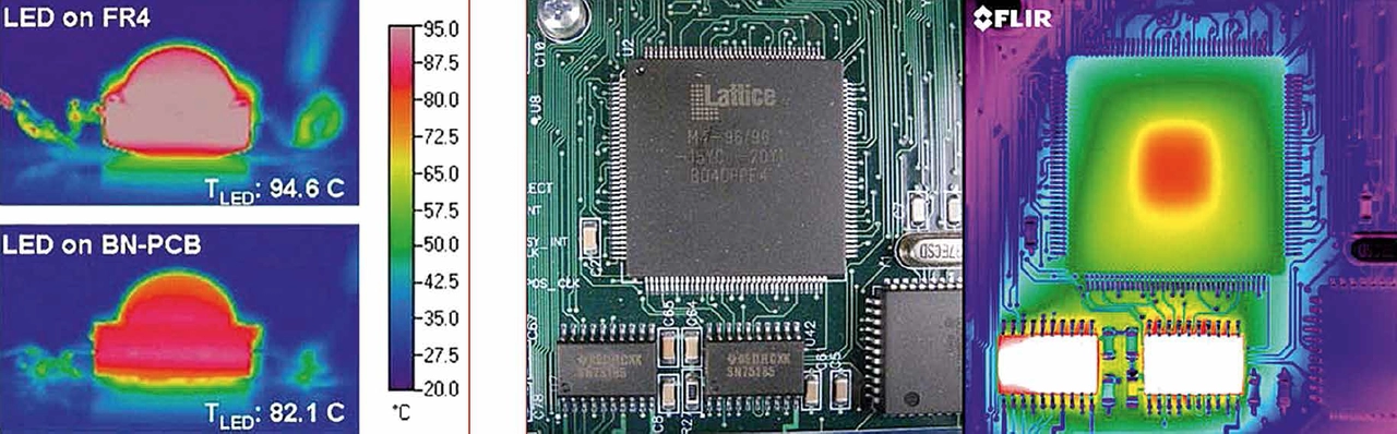
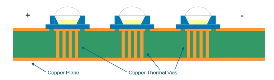
When it comes to efficient LED PCB via design, Via-in-Pad Plated Over (VIPPO) stands out. This technique enables direct heat transfer from the LED slug straight into the via, cutting down the thermal path length significantly. The manufacturing steps for VIPPO include:
- Drilling the via holes
- Plating the hole walls with copper
- Filling with resin or copper for stability and conductivity
- Capping to provide a smooth surface for LED soldering
This process not only boosts heat dissipation but also saves precious board space, making VIPPO ideal for high-density LED layouts.
Meanwhile, Blind and Buried Vias play a critical role in Metal Core PCBs (MCPCB) designed for LEDs. These vias allow multi-layer LED driver circuits to interconnect without penetrating the thermal dielectric layer, preserving heat conduction. Controlled depth drilling ensures these vias stop precisely where needed, maintaining the rigid thermal barrier crucial to LED junction temperature management.
| Technology | Key Benefits | Manufacturing Notes |
|---|---|---|
| VIPPO | Shorter thermal paths, space-saving | Drill → Plate → Fill → Cap |
| Blind/Buried Vias (MCPCB) | Maintain thermal integrity in multilayers | Depth-controlled drilling |
Incorporating these advanced interconnect methods improves thermal conduction and electrical reliability, supporting high-power LED applications. For a seamless LED driver circuit design tailored to these technologies, check out our comprehensive solutions on LED light driver PCB boards.
Manufacturing Variables Affecting Electrical & Thermal Reliability
When designing LED PCBs, certain manufacturing factors directly impact the electrical and thermal reliability of vias. Understanding these can help prevent failures, especially in high-power LED applications.
Tenting, Plugging, and Filling Vias
Tenting (covering via holes with solder mask) is a quick fix but often falls short for high-power LEDs. It can trap moisture and outgas during soldering, causing defects. For reliable thermal via arrays, plugging or filling the vias is more effective.
- Conductive fills like silver or copper pastes are used when vias need to carry high current or improve thermal conductivity, creating a direct heat dissipation path.
- Non-conductive epoxy fills work well when electrical isolation is crucial but still require solid mechanical and thermal support.
Choosing conductive vs. non-conductive via filling depends on balancing thermal performance and electrical isolation needs.
Solder Mask Dams
Solder mask dams are narrow barriers applied between vias and copper pads. They prevent solder from flowing away (“solder theft”) during reflow soldering, which can weaken the LED attachment or cause voids. Properly designed solder mask dams ensure consistent solder coverage and robust LED solder joints.
Surface Finishes and Via Flatness
Surface treatments like ENIG (Electroless Nickel Immersion Gold), HASL (Hot Air Solder Leveling), and OSP (Organic Solderability Preservatives) influence the flatness of the via surface. Flat via pads improve solder wetting and LED mounting stability. ENIG, while more expensive, is excellent for fine-pitch LEDs as it provides a very flat and stable surface—ideal for consistent LED junction temperature management over time.
For details on custom PCB layering and finishes that optimize LED reliability, check out our custom high-power aluminum LED PCB options.
Balancing these manufacturing variables enhances both thermal management and electrical integrity of your LED PCB vias to support long-term performance and durability.
Current Carrying Capacity and Inductance Considerations
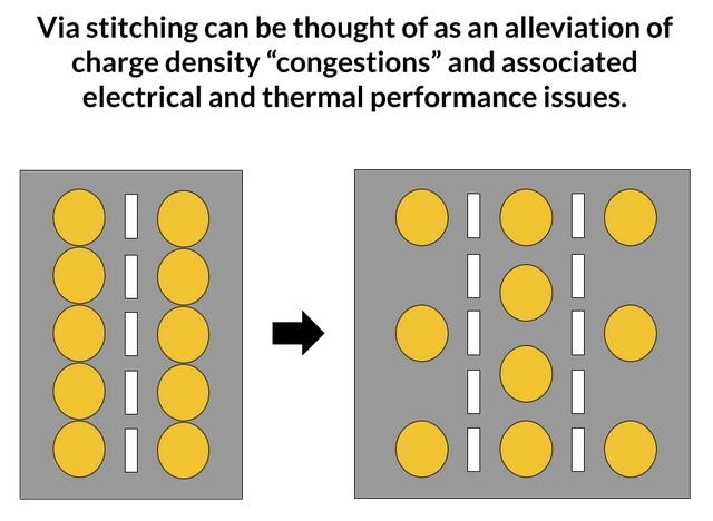
When designing LED PCBs for high-lumen COB (Chip on Board) arrays, managing current carrying capacity is crucial. The number of thermal vias directly impacts a board’s ability to handle significant current loads without overheating. As a rule of thumb, increasing via count lowers overall thermal resistance and spreads heat more effectively, preventing excess junction temperature rise that can degrade LED performance.
For high-current applications, each via’s size and plating thickness also play a part, but multiplying vias in an optimized array is often the most reliable method to safely carry large currents. This helps ensure consistent brightness and extends the LED life cycle by maintaining optimal thermal conditions.
On the electrical side, minimizing parasitic inductance from via structures becomes important in high-frequency LED driver circuits. Inductance can cause voltage spikes and adversely affect switching performance, leading to inefficiencies or even damage. To reduce this, designers should consider placing multiple smaller vias in parallel instead of a single large via, aligning vias close to component pads, and limiting via stub lengths.
Balancing via count, geometry, and layout enables a thermal via array that supports high lumens and stable driver functionality. For detailed thermal management and custom LED board solutions, check out our specialized insights on high-CRI LED PCB boards tailored for demanding applications.
Quality Control and Reliability Testing
Ensuring the reliability of LED PCB vias starts with thorough quality control checks during and after manufacturing. One critical step is cross-section analysis, which verifies the integrity of the via plating and the smoothness of the hole walls. This process helps catch voids, uneven copper thickness, or defects that could compromise thermal conductivity and mechanical strength.
Next, thermal stress testing like the Interconnect Stress Test (IST) is essential. IST exposes the PCB to repeated heating and cooling cycles to simulate real operating conditions. This step ensures vias maintain their structure and performance under thermal cycling, crucial for managing LED junction temperatures and preventing sudden failures.
For electrical reliability, flying probe testing is used to check continuity within complex via nets without damaging the board. This rapid, precise test identifies any open circuits or shorts across the plated through-hole (PTH) vias, assuring consistent current flow even in dense LED driver circuits.
Implementing these quality measures guarantees that thermal via arrays and other advanced interconnect technologies function reliably in demanding LED applications. For more insights on high-precision LED PCB assembly processes, you can explore resources such as detailed LED control PCB board assembly companies that specialize in optimizing via reliability in various LED designs.
Why Partner with China LED PCB
Choosing China LED PCB means you get more than just a manufacturer—you gain a partner with deep expertise in thermal management and LED PCB via design. Our team offers custom engineering support for thermal simulation, helping you optimize heat dissipation pathways before production. This proactive approach reduces LED junction temperature risks and enhances long-term reliability.
We specialize in handling a variety of substrate materials, including Aluminum Backed PCBs, Copper Core boards, and advanced FR4-Metal composites, tailored to your LED application needs. Whether you require precision thermal via arrays or robust Metal Core PCB (MCPCB) interconnects, our capabilities cover it all with consistent quality and IPC-6012 Class 3 plating standards.
Ready to improve your LED PCB design? Submit your Gerber files for a comprehensive DFM (Design for Manufacturability) review on thermal via placement and let our experts help you prevent overheating issues and ensure reliability. Learn more about our custom aluminum PCB LED lighting board options to see how we bring performance and cost-effectiveness together.
For deeper insight into high-performance LED PCB substrate options, explore our resources on advantages of aluminum LED PCBs tailored to enhance your next project.
 English
  Spanish
  French
  Portuguese
  Italian